TEM analysis
Transmission electron microscopy (TEM) uses an electron beam to form high-resolution images of objects – including their internal structures – on the nanoscale. TEM analysis is widely used in industries including materials science, microbiology, and nanotechnology.

Some of our TEM services
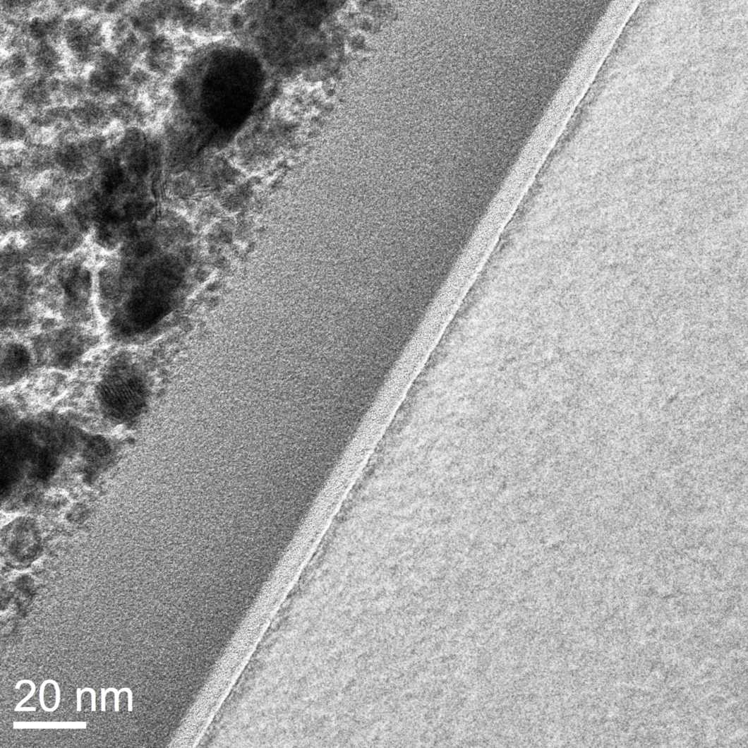
HR-TEM imaging
STEM-EDX
Particle size distribution with TEM
Negative staining TEM or cryo-TEM for liposomal powders
Prices excluding VAT.
Common applications of TEM analysis
The electronics industry and nanotechnology laboratories use TEM to examine thin film materials. The method is commonly applied to identify imperfections, failures, and (with EDX or EELS) impurities. TEM is also used for electron diffraction to determine the crystal structure of solid samples and reveal crystallographic orientations with high accuracy.
TEM enables the study of the internal structures of extremely small objects such as microbes and viruses, making it a widely used technique in medical and microbiological research (often with cryogenic preparation to reduce damage from the electron beam). In addition, TEM can be used to determine the particle size distribution of sub-50 nm nanoparticles and characterize nanomaterials in accordance with food according to EFSA guidelines.
How does TEM work?
The basic principle of transmission electron microscopy is similar to that of optical microscopy, but instead of light, TEM uses a transmitted electron beam that penetrates the sample. Because electrons have a smaller wavelength than light, the formed image has a considerably higher resolution compared to traditional light microscopy. The final image is highly detailed and shows the sample's internal structures. In some cases, it is even possible to distinguish individual atoms with TEM and its variation, STEM (scanning transmission electron microscopy).

Limitations of transmission electron microscopy
Despite the wide range of applications, TEM has some limitations. Samples must be electron-transparent, which means that sample thickness must be 100 nm or less. Larger samples can, however, be processed to fit the requirements. This can be achieved with the help of FIB sample preparation and cross-sectional TEM analysis, which focuses on studying sub-sections of particles that are too large for regular transmission electron microscopy.
TEM samples are also vulnerable to radiation damage from the electron beam. To counter this, fragile samples such as biological macromolecules can be pretreated by instant freezing and analyzed by cryo-TEM. Alternatively, negative staining pretreatment can be used for certain fragile sample types, such as liposome dispersions and powders.
If you're interested in the advantages and limitations of TEM compared to scanning electron microscopy, check out our expert article on the differences between SEM and TEM.
Our TEM analysis services
Measurlabs offers high-resolution imaging services with TEM, cross-sectional TEM, cryo-TEM, and STEM. If you already have detailed sample preparation and analysis protocols available, we will adhere to them precisely. Alternatively, our materials testing experts can help formulate the optimal testing strategy to match your samples and analytical goals.
For a practical example of our service in use, see the following case study:
For more information or a quote, please contact us using the form below.
Suitable sample matrices
- Materials in the nanoscale
- Nanoparticles
- Viruses and microbes
- Parts of semiconductors
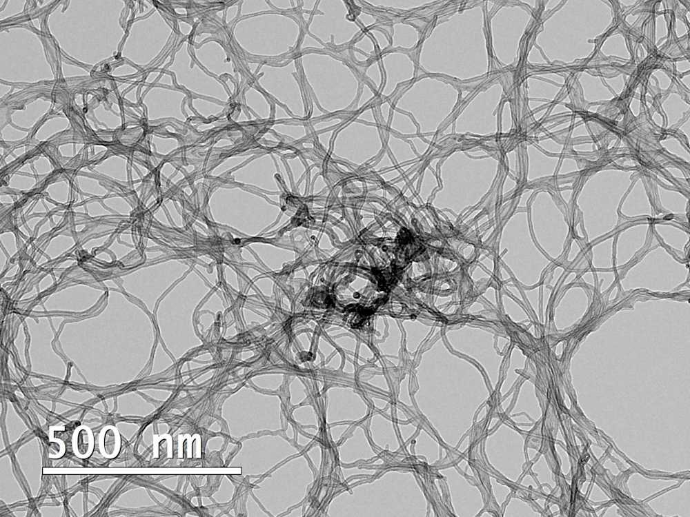
- Carbon nanotubes, graphenes and other carbon nanomaterials
- Thin film coatings
- Cellulose nanofibers
Ideal uses of TEM analysis
- Failure analysis in electronics manufacturing
- Imaging in materials science
- Studying the inner parts of microbes and viruses at an ultrastructural level
- Determining particle shape and size of nanoparticles
- Determining the location of catalyst particles in the carrier
- Imaging cellulose nanofibers
- Imaging carbon nanotubes, graphene, and other carbon nanomaterials
Ask for an offer
Fill in the form, and we'll reply in one business day.
Have questions or need help? Email us at info@measurlabs.com or call our sales team.
Frequently asked questions
TEM is mainly used in the fields of electronics and nanotechnology, but it can also be used in microbial research.
TEM produces high-resolution images that can be used in quality control and failure analysis. When combined with EELS or EDX, information on the elemental composition of the imaged sample can also be obtained.
Some materials cannot sustain the high-energy electron beam used in TEM. It may, however, be possible to analyze such fragile materials using cryo-TEM, where the sample is instantly frozen before analysis.
The TEM beam only passes through samples with thicknesses less than 100 nm. This requires thicker samples to be cut using techniques like microtomy or ion milling, making TEM a destructive method. Non-destructive alternatives in semiconductor failure analysis include micro-CT and scanning acoustic microscopy (SAM).
Measurlabs offers a variety of laboratory analyses for product developers and quality managers. We perform some of the analyses in our own lab, but mostly we outsource them to carefully selected partner laboratories. This way we can send each sample to the lab that is best suited for the purpose, and offer high-quality analyses with more than a thousand different methods to our clients.
When you contact us through our contact form or by email, one of our specialists will take ownership of your case and answer your query. You get an offer with all the necessary details about the analysis, and can send your samples to the indicated address. We will then take care of sending your samples to the correct laboratories and write a clear report on the results for you.
Samples are usually delivered to our laboratory via courier. Contact us for further details before sending samples.