X-ray photoelectron spectroscopy
X-ray photoelectron spectroscopy (XPS) is a technique for determining the elemental composition and chemical binding states of atoms on material surfaces. The method is applied widely across different industries to study materials ranging from semiconductors to engineering plastics.

Some of our XPS analysis services
X-ray photoelectron spectroscopy (XPS) depth profiling
X-ray photoelectron spectroscopy (XPS)
Prices excluding VAT.
What is XPS?
X-ray Photoelectron Spectroscopy (XPS), also known as Electron Spectroscopy for Chemical Analysis (ESCA), is a surface analysis technique used to determine the elemental composition and how those atoms are bonded. It can detect all elements except hydrogen (H) and helium (He) with a typical detection limit of 0.1 to 1 atomic%, depending on the element and sample material. XPS is very surface sensitive with a typical probing depth ranging between 3–9 nanometers (roughly 20-60 atom layers) or up to 300 nm with depth profiling.
XPS provides two key types of information:
Elemental composition: Which elements are present at the surface of a sample, and what are their concentrations.
Chemical states: How those elements are bonded (e.g., whether carbon is in a C–C, C–O, or C=O bond).
Because XPS can be used to characterize practically any solid and dry material, the technique is routinely used to study a plethora of different materials, such as semiconductors, metals, engineering plastics, coatings, catalysts, and fibers. Common applications include the determination of the atomic composition of thin films, catalyst studies, adhesive properties, wettability, corrosion, etc.
How does XPS work?
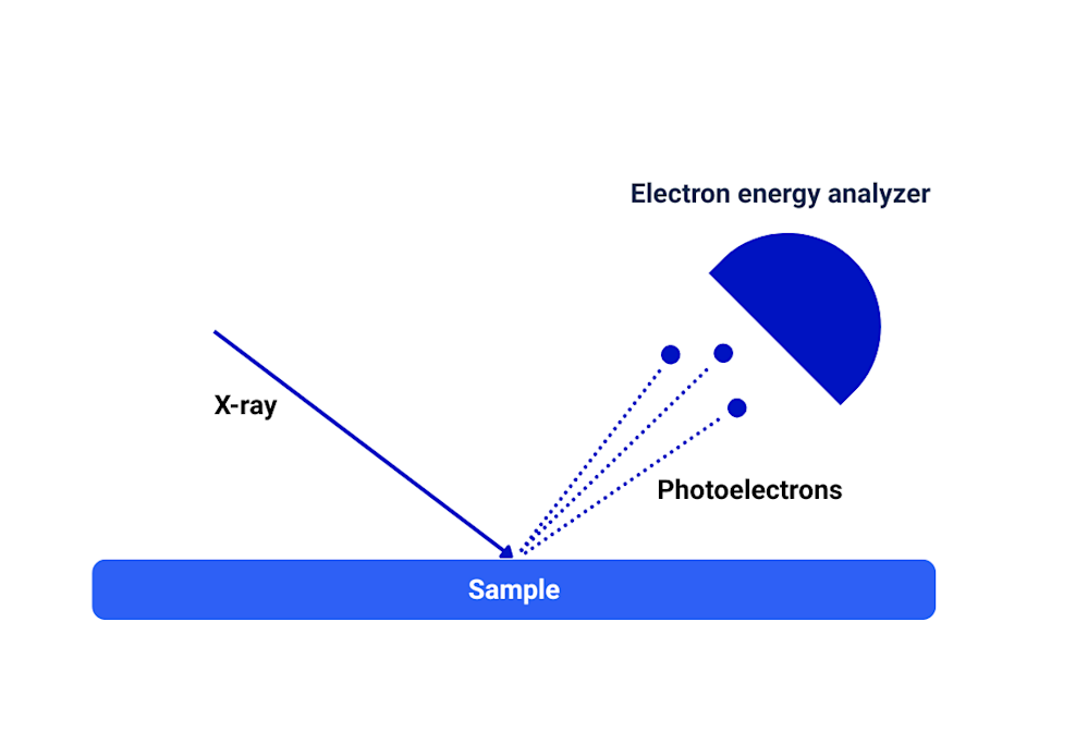
In XPS, the sample is bombarded with X-rays, which have enough energy to eject electrons from atoms on the material’s surface. These emitted electrons (called photoelectrons) have binding energies characteristic of their original atoms and the type of chemical bonds they were involved in. These binding energies are determined from the measured kinetic energies of the electrons and the known incident X-ray energy. By measuring the number and kinetic energies of the emitted photoelectrons, an XPS spectrum is generated. From this data, the following can be determined:
Which elements are present
Their relative amounts (atomic concentrations)
Their chemical environments (e.g., types of bonds)
How these characteristics change with depth (using a method called depth profiling).

XPS depth profiling
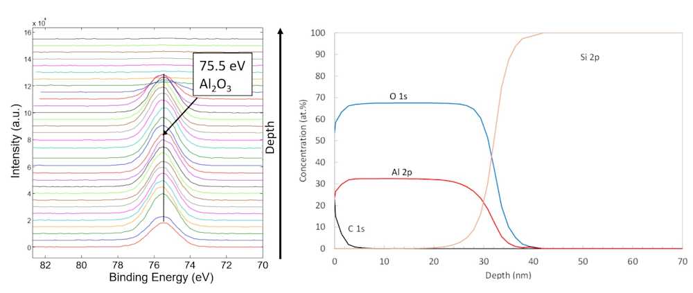
While XPS is very surface sensitive and the analysis depth is limited to just ~3-9 nm, depth profiling can be done by first performing an XPS measurement, then removing a known amount of material by charged ion etching (a process called ion sputtering), and then conducting another XPS analysis. By repeating this cycle many times, atomic depth profiles are attained.
During ion sputtering, the investigated material is bombarded with energetic charged ions, which etch the sample surface. Argon ions (Ar+), argon cluster ions (Arn+), or Buckminsterfullerene clusters (C60+) are commonly used to etch the material. Argon ion sputtering is commonly used for depth profiling metallic and ceramic materials that are resistant to etching, while argon cluster or Buckminsterfullerene cluster sputtering is used when the sample material is organic or otherwise sensitive to sputtering. Typically, ions with energy between 0.5 and 5 keV are used for sputtering, depending on the desired etching speed and the sample material.
By repeating XPS measurements and ion sputtering steps, depth profiling of surface layers ranging between 1 and 300 nanometers in thickness is possible with reasonable measurement times. In special cases, depth profiling can be done up to a micrometer depth.

Sample requirements and preparation
XPS samples must be dry and free of volatile compounds because the measurements are most commonly performed under ultra-high vacuum conditions. Suitable sample types include: Solids (e.g., thin films and bulk materials), powders, and coated surfaces
Typically preferred sample size is around 1 × 1 cm, though larger or smaller samples can often be accommodated. No special sample preparation steps are required for solid material samples that are free from volatiles, such as water or other solvents. Drying is needed for wet samples. Powder samples are fixed onto conductive carbon or copper tape or burnished onto conductive foil (e.g., indium).
Variations: lab-scale vs. synchrotron XPS
Typically, XPS measurements are conducted with laboratory-scale instruments, which offer cost-effectiveness and fast turnaround times. These devices use fixed energy X-ray sources (aluminium, magnesium, chromium, etc) with a limited intensity beam. This means that the energy of the X-ray beam cannot be altered to control the analysis depth, and the obtained spectral resolution and signal-to-noise ratio are only moderate.
The limitations of lab-scale XPS are usually irrelevant when the samples of interest consist of only a few chemically different phases, and probing the topmost few nanometers of the surface is enough. The limitations become relevant when analyzing samples consisting of numerous different phases with XPS peaks (energies of the emitted photoelectrons) close to each other or when a very small (< 3 nm) or large probing depth (> 10 nm) is sought.
Synchrotron XPS offers a significantly higher intensity primary X-ray beam than a lab-scale instrument. As a result, the spectral resolution of synchrotron-based XPS is remarkably better than that of a lab-scale instrument. The energy of the primary X-ray beam can be adjusted in a synchrotron setup. This enables adjusting the analysis depth from just a few nanometers to up to 30 nm or more. Due to these benefits, synchrotron-based XPS is often used when the samples consist of several phases and very detailed information on the bonding of the surface atoms is sought after. These benefits come with drawbacks also; turnaround times for synchrotron XPS are typically a bit longer, and prices are slightly higher compared to lab-scale XPS.
While most XPS measurements are conducted under ultra-high vacuum, which prohibits characterization of samples containing volatile compounds, the near ambient pressure XPS (NAP-XPS) setups, primarily available at synchrotron facilities, allow measurement of chemical changes in the sample surface in the presence of different dosed gases (H2O, N2, etc) at higher pressures (~30 mbar). This allows for in-situ studies of catalysis reactions, surface adsorption, corrosion, and the characterization of surface intermediates during the initial stages of ALD processes.
Limitations and supplementary methods
While XPS can be used to study various solid materials, it has certain limitations. First of all, the method is surface sensitive. If the elemental composition of bulk material should be analyzed, XRF offers a better solution. With XPS, the detection limit is typically around 0.1-1 atomic %. Therefore, the method is not suitable for trace contamination analysis, and other methods, such as VPD-ICP-MS, TXRF, SIMS, Tof-SIMS, or ATD-GC-MS, should be considered for that purpose. Another limitation of XPS is its inability to detect hydrogen (H). ToF-ERDA or SIMS should be used if the hydrogen concentration needs to be analyzed.
Need an analysis?
Measurlabs offers XPS testing services for various sample types, including thin films, metals, and organic materials. Through our partner laboratory network, we have access to several instruments (more details on our XPS service page, also synchrotron XPS is available) and can meet any requirements you have for both surface- and depth-profiling analysis needs. We can analyze even large sample batches with quick turnaround times – contact us through the form below to discuss with our experts and get a quote.
Method Expert
Suitable sample matrices
- Catalysts
- Thin films (ALD, CVD, PVD, etc)
- Semiconductors
- Plastics and plastic coatings
- Metals
- Glass
- Fibers and fiber composites
Ideal uses of XPS
- Defining the atomic stoichiometries of thin films
- Analyzing surface oxidation states post-production
- Catalyst studies
- Identifying surface impurities in metals, plastics, glass, and fibers
- Studying surface interactions
- Investigating corrosion, oxidation, nitriding, and carburizing in metals
- Evaluating impacts of lubricants, adhesives, and cleaners on surfaces
Ask for an offer
Fill in the form, and we'll reply in one business day.
Have questions or need help? Email us at info@measurlabs.com or call our sales team.
Frequently asked questions
Measurlabs offers a variety of laboratory analyses for product developers and quality managers. We perform some of the analyses in our own lab, but mostly we outsource them to carefully selected partner laboratories. This way we can send each sample to the lab that is best suited for the purpose, and offer high-quality analyses with more than a thousand different methods to our clients.
When you contact us through our contact form or by email, one of our specialists will take ownership of your case and answer your query. You get an offer with all the necessary details about the analysis, and can send your samples to the indicated address. We will then take care of sending your samples to the correct laboratories and write a clear report on the results for you.
Samples are usually delivered to our laboratory via courier. Contact us for further details before sending samples.
