SEM-EDX analysis
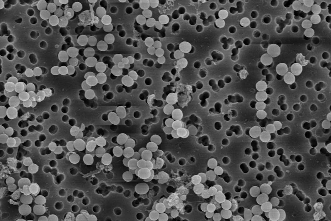
Scanning electron microscopy (SEM) with energy-dispersive X-ray spectroscopy (EDS or EDX) generates a sharp picture of the sample's microscopic surface structures and provides information about its elemental composition. SEM-EDX analysis is suitable for almost all sample types and has a vast number of applications from basic scientific research to product development and quality control.

Some of our SEM services
Prices excluding VAT.
What is SEM-EDX used for?
SEM-EDX has many applications in industrial manufacturing and materials science. It can also be used for energy and resource management, as well as for the examination of consumer-packaged goods. With SEM-EDX, large, heavy, and challenging samples can be examined with excellent image quality, showing the smallest details and the chemical composition of the material's surface.
In product development, SEM-EDX is commonly used for failure and defect analyses and process characterization. Particle type and size determination and material classification can also be performed with the help of SEM-EDX to ensure the quality of the product and optimize its production process. It is also possible to perform reverse engineering and breaking mechanism analyses.
Elemental mapping, where different elements and compounds detected by the EDX detector are marked with different colors in the picture, is an effective method for observing the elemental composition of a sample at a glance. SEM-EDX can also be used to determine whether the produced material contains additional substances, such as asbestos fibers. When the same analyses are performed on raw materials and process samples from different manufacturing stages, the most likely source and point of contamination can also be identified.
Deeper structural analysis of different materials with SEM-EDX can be very useful for research and development work. This includes examining surface topology, detecting surface contamination, and determining the causes of chemical reactions such as corrosion and oxidation.
How does SEM-EDX work?
With SEM, the microscopic surface structures of the sample can be observed with high precision. A scanning electron microscope typically has a resolution in the nanometer range, which is much higher than that of a traditional light microscope. Therefore, a more accurate image of the sample’s surface topography is obtained with SEM. More information about the SEM operating principle can be found on our SEM page.
A large selection of needs in science and industry can be met with SEM, as many different accessories can be added to the microscope to get different kinds of information about the sample (e.g., EBSD, BSE). When the goal is to determine the sample's elemental composition, an additional EDX detector is attached to the SEM machine. The EDX detector identifies the elements in the sample along with their concentrations and distribution.
The operating principle of EDX
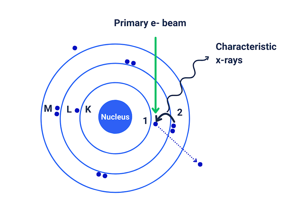
The EDX detector detects the X-rays that are produced by the material when electrons interact with its surface during SEM imaging. EDX analyzes the X-rays and can therefore identify all other elements in the sample except for hydrogen, helium, and lithium. The elements can be distinguished from each other because every element has its own kind of X-ray spectrum, which they emit after interacting with the electrons. This information about different spectra from different parts of the sample can be visualized, for example, in an elemental map of the sample’s surface where different elements and compounds have been marked with different colors.

More information about the interaction happening in the sample can be found on our XRF page. In X-ray fluorescence (XRF), the same phenomenon is utilized to identify elements as in SEM-EDX, but with the help of X-rays instead of electrons. Another similar technique is electron energy loss spectroscopy (EELS), which is most often conducted together with TEM or STEM.
Need SEM-EDX analyses?
Measurlabs offers laboratory testing with SEM and SEM-EDX techniques for a variety of samples and analytical needs. We combine competitive pricing with short turnaround times to help your projects advance as smoothly as possible. Our expert support and broad portfolio of additional analysis techniques make it easy to streamline testing procurement and save time. Contact us through the form below to request a custom quote and start the discussion with our team.
Suitable sample matrices
- Solid samples
- Powders
- Different materials, such as metals or polymers
Ideal uses of SEM-EDX
- Identification of different elements and determination of their concentrations and distribution in specific areas of the sample’s surface
- Clarifying the causes of chemical reactions through elemental mapping
- Defect analysis, process characterization, analysis of breaking mechanisms, and particle identification
- Finding contaminants that do not belong in the target material
- Study of complex environmental and biological samples to find out the structures and compositions of their surfaces
Ask for an offer
Fill in the form, and we'll reply in one business day.
Have questions or need help? Email us at info@measurlabs.com or call our sales team.
Frequently asked questions
Some common applications of SEM-EDX include failure analysis and production process optimization, as the combination of SEM with the EDX detector enables the detection of both structural issues and chemical contaminants. The method can also be used to identify particles and their size distributions, examine surface topology, and determine the causes of detrimental chemical reactions like corrosion and oxidation.
Only the surface structures of the sample can be examined with SEM if the sample and its inner parts are to be kept in one piece and undamaged. If the sample is too large for the microscope, it may need some cutting (for example with the focused ion beam) before analysis. Other sample preparation techniques are often needed if the sample is dirty or wet, or if it does not conduct electricity.
The analysis and possible coating of the sample in SEM-EDX may also limit possible subsequent analyses. Some elemental peaks can overlap in the X-ray spectrum of the sample, which means that a thorough analysis of the results is needed to distinguish the elements from each other accurately. It also has to be acknowledged that hydrogen, helium, and lithium can not be detected with EDX. The size of the area analyzed with SEM-EDX ranges from approximately 0.1 to 3 micrometers.
Solid samples can be analyzed with SEM-EDX. If the sample is dry and conducts electricity, SEM-EDX does not require pretreatment of the sample and does not damage the material. If the sample does not meet these requirements, it must often be prepared before SEM: cleaning, fixing, drying, attaching to a platform, and coating with metal or carbon has to be performed before imaging.
Measurlabs offers a variety of laboratory analyses for product developers and quality managers. We perform some of the analyses in our own lab, but mostly we outsource them to carefully selected partner laboratories. This way we can send each sample to the lab that is best suited for the purpose, and offer high-quality analyses with more than a thousand different methods to our clients.
When you contact us through our contact form or by email, one of our specialists will take ownership of your case and answer your query. You get an offer with all the necessary details about the analysis, and can send your samples to the indicated address. We will then take care of sending your samples to the correct laboratories and write a clear report on the results for you.
Samples are usually delivered to our laboratory via courier. Contact us for further details before sending samples.