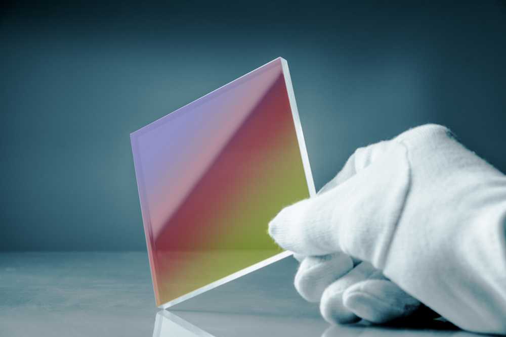
Thickness is one of the fundamental characteristics of thin films and affects their electrical, mechanical, and optical properties. Analyzing the thin film thickness is a critical part of product development in various industries and applications like semiconductors, displays, medical devices, and electronics.
The thickness can be analyzed with several different methods, like XRR, cross-sectional SEM, cross-sectional TEM, and ellipsometry. The selection is not always straightforward, and in this article, we will discuss the benefits and limitations of these methods and give insights on what factors to consider when making the selection.
Why is method selection so complex?
The complexity of method selection arises from the limitations of the methods and their varying capabilities to answer different research questions about the material. That is why there is seldom a single correct answer for which method is the best. Instead, it depends on what methods are eligible for the material in question, what additional information other than the thickness of the film is to be determined with the analysis, and what the budget is.
The factors that affect what methods are eligible for the material are the surface roughness of the film, the thickness range, and the material of the film and the substrate. These things thus need to be known at least approximately when selecting the method. The limitations of XRR, SEM, TEM, and ellipsometry are presented in the sections below.
Additional information that can be obtained with the thickness analysis is, for example, density, surface roughness, refractive index, and structural properties. For each method presented below, such additional information is also mentioned to facilitate making the correct selection.
Thickness measurements with XRR
X-ray reflectivity is a great method for the analysis of layered materials. It allows not only the determination of the thickness of the film in total but also gives information about the thickness and density of the individual layers in it. Surface roughness can also be measured as part of the thickness measurement with XRR.
The method is suitable for materials with a thickness smaller than 250 nm, optimally under 100 nm. For successful measurements, the thickness of the material must be at least one order of magnitude greater than the surface roughness of the film.
An important factor related to XRR is that the estimated composition and structure of the sample must be known for the analysis to be accurate. As the method relies on fitting the experimental XRR curve with the corresponding layer model using simulation, the analysis can result in large errors if the composition of the sample is unknown.
Thickness measurements with cross-sectional SEM
Scanning electron microscopy is a great method for analyzing the thickness of semiconductive thin films. SEM works for both single- and multi-layer materials, and can in addition to the thickness also provide information about the surface morphology and elemental composition of the sample.
The method is suitable for conductive and semiconductive materials with a thickness between 100 nm and 100 μm. Non-conductive materials can be analyzed with the method if the sample is prepared by depositing a thin layer of conductive material on the surface.
It is good to note that for results on the elemental composition of the film, an SEM equipped with an EDS detector (energy dispersive spectroscopy) is required. The EDS detector measures the x-rays emitted from the sample when the electrons interact with it. As the detector analyses the X-ray spectrum, it recognizes the spectrums of individual elements and compounds and allows for their identification and quantification.
Thickness measurements with cross-sectional TEM
Transmission electron microscopy is another method commonly used for analyzing conductive and semiconductive films. This method also works for both single- and multilayer materials in the thickness range of a few nanometers to 100 nm. Suitable sample thickness can be achieved using the focused ion beam (FIB).
Similarly to cross-sectional SEM, an EDS detector can also be attached to the TEM to obtain information about the elemental composition of the sample. With TEM you can also get valuable insight into the structure of the sample. The method thus offers a lot of information about the material, but the analyses are also clearly more expensive than the measurements done with SEM.
An important risk to consider with TEM is that the high-voltage beam can burn and harm some materials. For example for polymeric and organic materials, the suitability of the material should be carefully considered before starting the analysis.
Thickness measurements with ellipsometry
Spectroscopic ellipsometry is a commonly used method for thickness measurements of transparent and semitransparent single- and multilayer films. The thickness range where this method is suitable is between 1 nm and 1,000 nm.
Ellipsometry also allows calculating the refractive index of the film. The refractive index is the ratio of the velocity of light in a vacuum to its velocity in a specified medium and gives information about how the material interacts with light passing through it.
Conclusions
To conclude, there are a few factors affecting the method selection for thin film thickness measurements, and no absolute rules for when to go with which one. The thickness of the film is one clear factor that limits the methods available, but otherwise, the selection is widely dependent on the context of the analysis. The selection should be made with the sample and the aim of the project in mind to ensure that the collected information responds to the research question in the best possible way.
Further reading about the working principles and ideal uses of the mentioned methods:
Read more about x-ray reflectivity method
Read more about scanning electron microscopy and SEM-EDX method
Read more about cross-sectional transmission electron microscopy
Read more about spectroscopic ellipsometry method

