TXRF analysis
Total reflection X-ray fluorescence (TXRF) is an elemental analysis technique used to detect ultra-trace levels of elemental contamination on smooth, flat surfaces. It is mainly used in the semiconductor industry to analyze metallic contaminants on wafers during process development and routine production.

What is TXRF analysis used for?
TXRF is mainly used to study metallic contamination on wafers in the semiconductor industry. The technique can detect elements from sodium (Na) to uranium (U) at surface concentrations between 109 and 1012 atoms per square centimeter, making it one of the most sensitive methods for surface trace contamination studies.
Working principle and results of TXRF
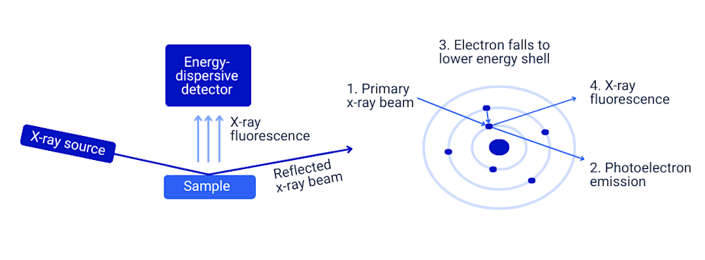
The operating principle of TXRF and the underlying X-ray fluorescence are illustrated in Figure 1. TXRF analysis begins by generating a monochromatic X-ray beam, which is directed at the surface of a sample at a very shallow angle, usually less than 0.5° with respect to the plane of the surface. This means that the beam only penetrates to the very surface of the sample (~5 nm), and the underlying structures do not hamper the surface analysis.
As the X-ray beam hits the surface, it excites the atoms on the surface by removing low-energy state electrons from their inner electron shells. A higher energy electron from an outer electron shell then falls to the inner electron shell to fill the vacancy. This falling of the electron to the inner shell results in the release of secondary X-rays (X-ray fluorescence). These secondary X-rays have distinct energies based on the atoms from which they are emitted. Detection of the secondary X-rays with an energy-dispersive detector enables the determination of the particular elements and their concentrations in the sample.

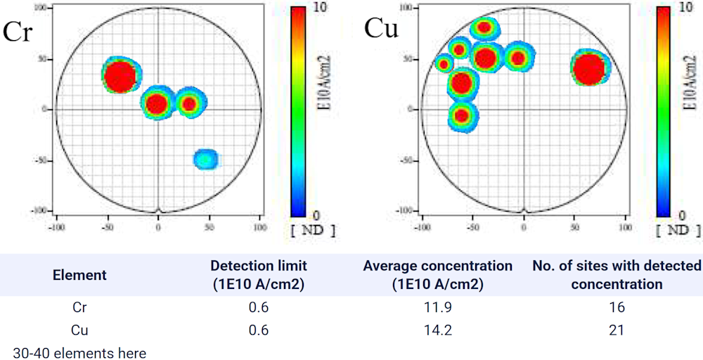
In a typical TXRF setup, one wafer is subjected to 40–300 TXRF measurements from individual spots, and the concentrations of different impurity elements are then plotted as two-dimensional heat maps (Figure 2 below).

Suitable samples and use cases
TXRF is suitable for bare and coated wafers with 100–300 mm sizes. Practically all common wafer materials, such as Si, SiC, GaAs, GaN, InP, and glass, are suitable for TXRF. The main requirement for TXRF analysis is a smooth surface, so wafers with thin films grown with typical deposition methods, such as ALD, CVD, PVD, or similar, can be studied.
TXRF is a non-destructive method, so it allows wafers to be analyzed both before and after specific fabrication steps. This enables contamination source tracking during semiconductor processing. For instance, if a wafer shows negligible contamination before transport within the fabrication facility, but exhibits localized iron (Fe), chromium (Cr), and nickel (Ni) near the edges afterward, a stainless steel wafer clamp used during transport could be identified as a likely source of the contamination.
Considerations and alternative methods
Due to the extreme sensitivity of TXRF for elemental impurities, all samples sent to TXRF analysis need to be carefully packed into a wafer carrier or FOUP and sealed in airtight packages in a cleanroom to avoid contamination during transport.
While TXRF is a very powerful tool for determining the metallic impurities on the wafers and the mapping offering unique opportunities in identifying the contamination sources in the production process, the method is among the most costly ones used for contamination analysis. Mapping of an individual wafer typically costs somewhere between €1,000 and €10,000, depending on the wafer size, number of points measured, and the number of samples.
When seeking a routine method for surface elemental contamination studies of wafers, VPD-ICP-MS (vapor phase decomposition-inductively coupled plasma-mass spectrometry) offers a cost-effective alternative for TXRF with even lower detection limits. However, the location information of contamination cannot be achieved with VPD-ICP-MS. Both TXRF and VPD-ICP-MS are surface sensitive, so other methods, such as SIMS (secondary ion mass spectrometry), need to be used if elemental depth profiling is sought after. When organic contamination is studied, ATD GC-MS (automated thermal desorption-gas chromatography-mass spectrometry) is the method of choice.
TXRF vs XRF
Fundamentally, X-ray fluorescence (XRF) and TXRF work in the same way. The difference arises as the TXRF setup is designed specifically to reduce the amount of scattered and absorbed X-rays, instead maximizing the amount of fluorescence. This, in turn, produces a very high signal-to-noise ratio and allows the technique to have a far higher sensitivity than conventional XRF.
The main disadvantages of TXRF compared to conventional XRF are the expensive and large instrumentation required for the former. TXRF also requires completely smooth samples with no particulate impurities on the samples, while XRF can be used to analyze almost any type of solid or liquid samples without smoothness or cleanliness requirements. Due to these differences, XRF can be used to study the elemental composition and impurities of various samples with minimal sample prep and precautions, while TXRF is practically only applicable in the semiconductor industry.
Need TXRF analyses?
Measurlabs offers laboratory testing with TXRF, as well as several other techniques (ToF-SIMS, VPD-ICP-MS, etc.) for trace-level contamination analysis of thin films and wafers. We have options for express turnaround times for time-critical projects and can handle large sample batches efficiently. Thanks to our comprehensive range of techniques, you can access all the analyses you need through one partner. Contact our experts using the form below to get a quote.
Method Expert
Suitable sample matrices
- Wafers (Si, SiC, GaAs, GaN, InP, etc.)
- Thin films
- Semiconductors
Ideal uses of TXRF
- Trace element detection
- Wafer mapping
- Contamination source tracking
Ask for an offer
Fill in the form, and we'll reply in one business day.
Have questions or need help? Email us at info@measurlabs.com or call our sales team.
Frequently asked questions
Measurlabs offers a variety of laboratory analyses for product developers and quality managers. We perform some of the analyses in our own lab, but mostly we outsource them to carefully selected partner laboratories. This way we can send each sample to the lab that is best suited for the purpose, and offer high-quality analyses with more than a thousand different methods to our clients.
When you contact us through our contact form or by email, one of our specialists will take ownership of your case and answer your query. You get an offer with all the necessary details about the analysis, and can send your samples to the indicated address. We will then take care of sending your samples to the correct laboratories and write a clear report on the results for you.
Samples are usually delivered to our laboratory via courier. Contact us for further details before sending samples.
