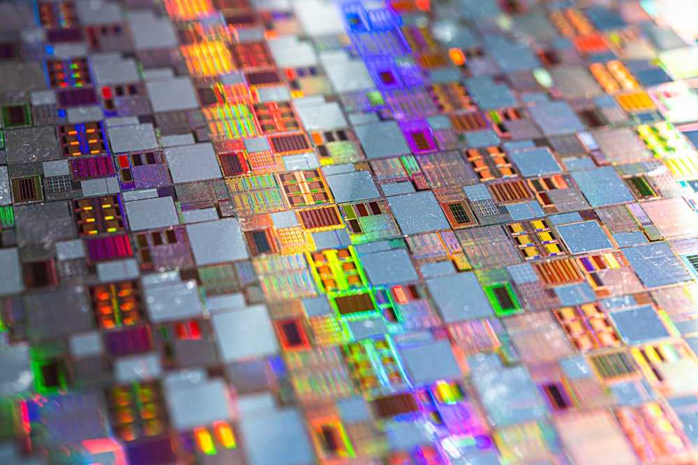
In modern semiconductor applications, even small ultra-trace concentrations of contaminants (<1 ppm) can compromise the device's operation. This makes trace elemental analysis (TEA) indispensable to quality assurance and new material research and development.
Choosing the most suitable trace elemental analysis technique
Several analytical techniques can be used to detect elemental impurities at trace and ultra-trace levels, but there are crucial differences in their applicability and target elements that are important to know to select a proper analytical solution. The factors to consider during method selection include:
Elements of interest: Most TEA techniques can detect metallic elements. Fewer methods are available for the analysis of light elements or organic impurities.
Required sensitivity: While ppm-level can be reached with a larger number of techniques, the options are considerably more limited when ppb-level detection is required.
Area of interest: Some techniques survey the surface of the material as a whole, while others can map trace elements at specified locations across the surface or as a function of depth.
Table 1 summarises four popular analysis techniques for trace element detection. More information on each method is provided further on.
Table 1: Comparison of selected trace elemental analysis techniques
Technique | Sensitivity | Applications | Detection capabilities |
ICP-MS-based methods | ppm - ppb 107–109 at/cm2 | Full wafer surface analysis | Most elements except H, C, N, O, F |
TXRF (or VPD-TXRF) | 109–1011 at/cm2 | Surface analysis (mapping) | Na to U |
SIMS and ToF-SIMS | ppm - ppb | Surface analysis & depth profiling | All elements |
ATD GC-MS | pg/cm2 | Full wafer analysis | Organic contaminants: C7-C30 chained chemicals |
ICP-MS for ppb level surface contaminant analysis
VPD-ICP-MS (vapor phase decomposition-inductively coupled plasma-mass spectrometry) is a variation of the ICP-MS method ideal for detecting ultra-trace amounts of metal contaminants on the surfaces of silicon wafers and thin films. The method is based on using acid (usually HF) to dissolve the top layer of the film for analysis with ICP-MS and is mainly used for Si wafers and oxide thin films.
Other techniques based on ICP-MS, such as surface scanning or layer stripping, can reach similar detection limits and are more adapted to analyze thin films.
A standard ICP-MS measurement usually covers a package of metallic elements. Detection limits are different for different metals, ranging from approximately 107 at/cm2 to 109 at/cm2. Noble metal analysis options are also available, with the most typical target metals being Pd, Ag, Pt, and Au.
Compared to other semiconductor TEA techniques, VPD-ICP-MS is a relatively affordable solution to get the average trace contamination levels on the full surface of a wafer.
TXRF for trace element mapping
TXRF (total reflection X-ray fluorescence) is a highly sensitive variation of the XRF method, able to detect most metals at sensitivity ranging from 1010 to 1011 at/cm2. The analysis focuses on the extreme surface of the sample since it is done at a grazing angle. Three different X-ray energies are usually used to cover most of the elements.
TXRF analysis can be performed on full semiconductor wafers measuring up to 300 mm. It is possible to map the locations of impurities across the surface of the wafer. A key advantage of TXRF in trace elemental analysis is the minimization of matrix effects. Limitations include the inability to accurately detect elements with an atomic number below 11 and low sensitivity for Na, Mg, and Al. The surface of the analyzed film also needs to be smooth.
The combination of VPD and TXRF can improve the detection limit of TXRF and be useful in very specific cases where ICP-MS is not an option.
The pricing of TXRF measurements depends on several factors. If trace elemental mapping is performed, the price increases with the number of mapped points and the number of beams needed to detect the target elements.
SIMS for trace element depth profiling
SIMS (secondary ion mass spectrometry) or dynamic SIMS is a depth profiling method that can measure all elements from hydrogen to uranium down to ppm - ppb level. Not all elements can be measured simultaneously, and matrix-specific reference standards are required to obtain quantitative results. Most of the time, the technique is used to quantify dopants or trace contaminants.
ToF-SIMS (time-of-flight secondary ion mass spectrometry), also called static SIMS, is another good technique to measure trace contaminants. It has the advantage of having a sub-nm probing depth, which enables very accurate depth profiling.
ATD GC-MS for organic contamination analysis
ATD GC-MS (automated thermal desorption-gas chromatography-mass spectrometry) is a technique used to measure organic compounds. It can identify compounds as well as determine their concentrations in picogram quantities. The technique is particularly useful for identifying organic contaminants adsorbed on wafers or vapors that outgas from coatings.
All trace elemental analyses in one place
Measurlabs provides trace elemental analysis services for thin films, silicon wafers, and other semiconductor components using the techniques described above – and more. Our experts can also assist with method selection, so do not hesitate to contact us if you have any questions or wish to request a quote.

