Vapour phase decomposition ICP-MS
Vapor phase decomposition-inductively coupled plasma-mass spectrometry (VPD ICP-MS) is a combined sample preparation (VPD) and analysis technique (ICP-MS) that is used to determine the ultra-trace level concentration of metallic contaminants on the surface of wafers and thin films.

What is VPD ICP-MS, and what is it used for?
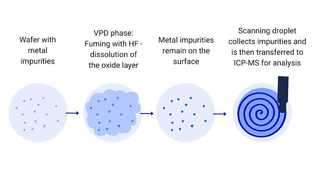
Vapor phase decomposition (VPD) is a sample preparation method that dissolves any metallic impurities on a smooth surface into a droplet of an acid solution. This allows for the extraction of said impurities, making them far easier to detect and identify, even when only present in ultra-trace amounts. ICP-MS is the analysis technique where the impurities are ionized and identified according to their masses.
VPD ICP-MS is used to analyze the surfaces of wafers and thin films in order to detect trace amounts of metal contamination. Metal contamination of semiconductors can severely impact their usability; hence, this is an essential technique for monitoring and controlling wafer quality.
The VPD method is very powerful because it allows the analysis of the whole surface of the wafer. This works well in conjunction with ICP-MS, which itself is ideal for detecting and quantifying very small amounts of metal impurities. The detection limit can go down to 106 at/cm2 for some elements.
VPD ICP-MS is suitable for bare and coated wafers with 100-300 mm sizes. Common wafer materials, such as Si, SiC, and borosilicate, are suitable for VPD ICP-MS. Bare wafers, wafers with native oxide layer, and wafers with thin films grown with typical deposition methods, such as ALD, CVD, PVD, or similar, can be studied.
It is important to emphasize that the method only focuses on the top few Angstroms of the topmost layer. For bulk contamination analysis of thin films, other sample preparation methods coupled with ICP-MS should be applied, such as film stripping. Please contact us for more information on bulk contamination analysis of thin films.
How does VPD-ICP-MS work?
The VPD process begins by exposing the surface of the substrate, usually a silicon wafer, to hydrofluoric acid vapor. This removes the topmost layer on the surface of the wafer and dissolves any metallic impurities. The surface of the wafer is then scanned with a droplet of scanning solution. This effectively picks up the impurities into a single droplet.

The next step of the analysis is performed using inductively coupled plasma-mass spectrometry (ICP-MS). The liquid sample gathered from the VPD is injected into the device. Here, the sample is decomposed and ionized by plasma, before being passed into a vacuum chamber. The ions accelerate along the length of the chamber, where they are separated by their respective charges and masses. A mass spectrometer is used to detect and quantify the ions to distinguish different elements.
The mass spectrometer data is converted to elemental concentration with the help of calibration curves for each element of interest. The elemental concentration (in at/cm2 ) and the detection limit per element are reported. To see what this looks like in practice, see our example report: VPD ICP-MS.
VPD ICP-MS vs TXRF: what is the difference?
Both VPD ICP-MS and TXRF offer trace contamination analysis on wafers, but they operate on different principles and have their own advantages and limitations. While VPD ICP-MS offers a cost-effective solution for routine contamination analyses, the method is inherently destructive due to the usage of acid solutions, unlike non-destructive TXRF. TXRF cannot detect elements with low atomic numbers because their fluorescent signals are too weak; VPD ICP-MS, on the other hand, is very sensitive to these elements. VPD ICP-MS has a superior detection limit of 106 - 1010 at/cm2, compared to TXRF’s detection limit of 109 - 1012. VPD ICP-MS yields a total contamination concentration without spatial data, whereas TXRF enables contaminant mapping by analyzing numerous points across the wafer surface.
Sample requirements and preparation
The surface of the wafer must dissolve readily in the hydrofluoric acid vapor, as the first step of VPD is dissolving the topmost layer with the HF vapor. In most cases, the surface of the wafer is composed of a sacrificial oxide layer, so this is no issue.
Once the VPD process is completed, the sample is analyzed through ICP-MS. This is a highly responsive technique that can be used on a wide range of subject matter. In terms of contaminants, most metals and some metalloids and nonmetals can be analyzed.
Quality control and contamination prevention
VPD ICP-MS is an ultra-sensitive analytical technique that demands a pristine, contamination-free environment to achieve accurate results. Stringent quality control measures should be implemented to ensure the highest data quality and prevent cross-contamination during the analysis. Bare wafers and wafers with thin films should be separated to further mitigate the risk of contamination. The cleanliness of the decomposition chamber and the surrounding environment should be actively monitored and verified with each set of wafers. One way to achieve this is to concurrently analyze wafer controls alongside the actual wafer samples, confirming the integrity of the analytical conditions for every run.
Need VDP ICP-MS analyses?
Measurlabs offers high-quality VDP ICP-MS analyses with short turnaround times and competitive prices for large or recurring orders. We handle large sample batches efficiently and can also offer any other analysis techniques needed for the quality control and R&D of thin films. Contact us through the form below to get a custom quote and start saving time in laboratory testing.
Suitable sample matrices
- Si, SiC, borosilicate wafers (bare or with native oxide films)
- Thin films that are soluble in hydrofluoric acid
- Other semiconductor materials
- Solid materials where surface trace metal contamination is of interest
Ideal uses of VPD ICP-MS
- Quantification ultra-trace metallic contamination on the bulk surface of wafers.
- Monitoring the cleanliness of semiconductor manufacturing processes and equipment.
- Identification of the sources of contamination that can affect semiconductor device quality and performance.
- Measurement of light element contaminants (e.g., sodium, potassium, calcium) where other techniques may be less effective.
Ask for an offer
Fill in the form, and we'll reply in one business day.
Have questions or need help? Email us at info@measurlabs.com or call our sales team.
Frequently asked questions
Measurlabs offers a variety of laboratory analyses for product developers and quality managers. We perform some of the analyses in our own lab, but mostly we outsource them to carefully selected partner laboratories. This way we can send each sample to the lab that is best suited for the purpose, and offer high-quality analyses with more than a thousand different methods to our clients.
When you contact us through our contact form or by email, one of our specialists will take ownership of your case and answer your query. You get an offer with all the necessary details about the analysis, and can send your samples to the indicated address. We will then take care of sending your samples to the correct laboratories and write a clear report on the results for you.
Samples are usually delivered to our laboratory via courier. Contact us for further details before sending samples.