Surface roughness is a crucial property that influences material durability and performance. For thin films and semiconductor devices, surface roughness is important for optimizing electrical properties, adhesion, and particle trapping, among other properties.
Method selection considerations
Different methods can be used to measure the roughness. Below are some considerations to help in selecting the most appropriate method:
Is a contact or non-contact method preferred? Or how precisely does the roughness need to be investigated?
Contact methods will provide a mapping of the roughness
Non-contact methods will provide the average roughness
How large is the area to be measured?
What resolution is needed?
Are you looking for more information? (thickness, interface roughness, density, Young's modulus, etc.)

Surface roughness measurement techniques
Many techniques can be used to measure the surface roughness of semiconductor components. A few of them are outlined below:
Atomic force microscopy (AFM)
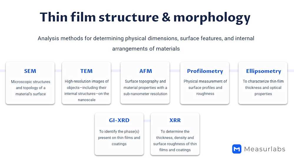
AFM is a very popular and versatile technique for measuring the surface roughness of a wide range of materials. It can be operated in contact or tapping mode, and it provides a topographic map of the surface with nanoscale resolution. AFM also allows measuring the elasticity and plasticity of the surface (Young's modulus). There are different AFM tools allowing measurements of additional properties; for example, EFM and C-AFM can give additional information on electrical properties.
X-ray reflectivity (XRR)
XRR is a non-contact technique that allows the determination of the surface roughness, as well as film thickness and density. It can probe a stack of thin layers of different materials and provide the roughness at the interface and surface, as well as their respective thicknesses and densities. XRR's resolution is 1% of the result, and the roughness provided is the average on the area analyzed, usually a few mm in diameter. XRR is particularly well-suited for low-roughness materials. Several points can be measured to map samples, such as wafers.
Profilometry and optical profilometry
Optical profilometry is a non-contact method, whereas profilometry is a contact method that uses a stylus to scan the surface and provides a topography mapping with nanoscale resolution. Both can be used for a wide variety of samples and have the advantage of easily measuring much larger areas than AFM. Optical profilometry is usually a much quicker solution than traditional profilometry.
One partner for all your thin film testing needs
Measurlabs offers AFM, XRR, profilometry, and several additional methods to analyze thin films and semiconductor surfaces. More information—including indicative pricing—about some of the most popular services can be found through the links below:
If you're unsure about which technique might be best for you, our experts are happy to help you select the most suitable option. Tell us about your samples and analysis goals using the form below, and we'll prepare a tailored offer. Remember to specify expected sample volumes, as we offer discounted rates for large and recurring orders.

