Scanning acoustic microscopy
Scanning acoustic microscopy (SAM or C-SAM) is a micro-imaging technique used to analyze fractures, delaminations, and other defects in various types of materials, including semiconductors, microelectronics, and biological samples.

What is scanning acoustic microscopy used for?
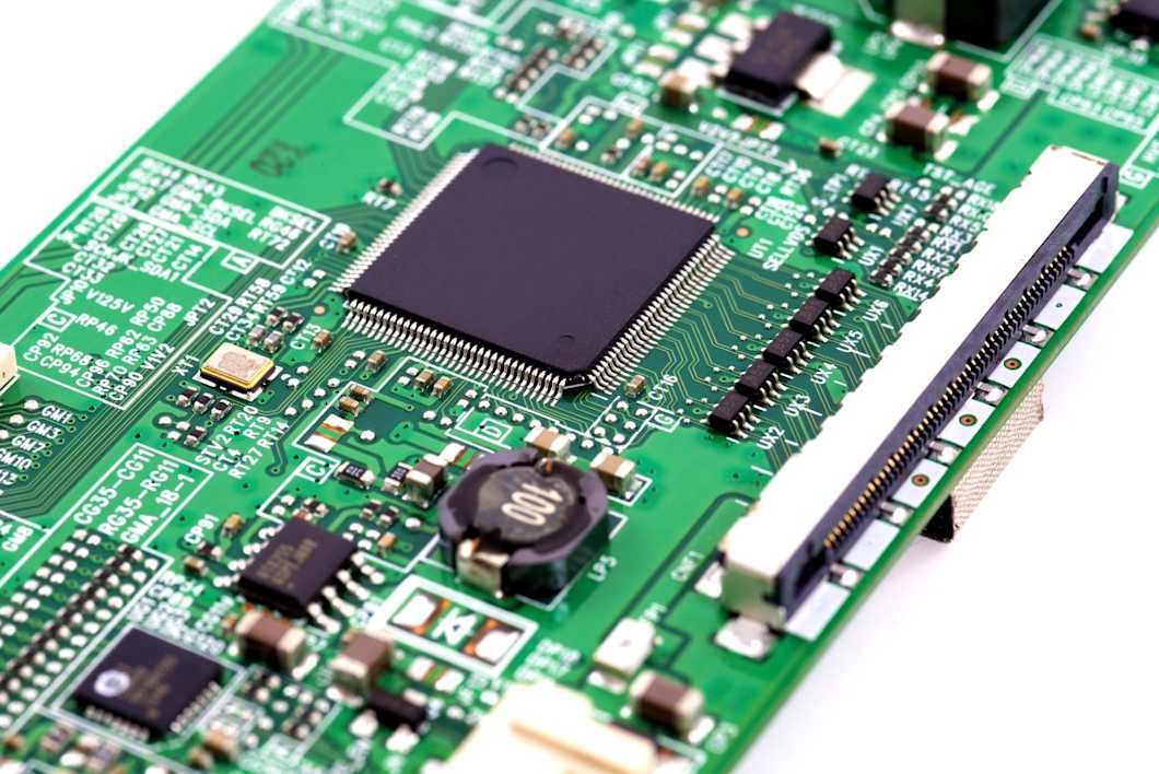
SAM (also known as ultrasonic microscopy and C-SAM, or confocal scanning acoustic microscopy) is a common failure analysis method in materials science. It is used for quality control and development of microelectronic components, including those encased in plastic, printed circuit boards, and silicon wafers. SAM is also used in microbiological studies to image cell and tissue properties.
In semiconductor testing, SAM can provide information on die-attach integrity, the presence of voids and cracks, the efficiency of bonding processes including solder efficiency, the integrity and uniformity of sealing, coating, and flip-chip underfills, the quality of wafer-to-wafer bonding, and the evaluation of solder bump integrity and alignment.
How does SAM microscopy work?
In SAM, ultrasound waves are fired at a fine point on a sample. These will interact with the materials and are either transmitted or reflected as they pass through different material boundaries. The resultant waves are detected, and any changes they exhibit are recorded. This process is repeated and used to build up an image of the material based on changes in acoustic impedance resulting from changes in density, refractive index, and phase changes between material boundaries.
Suitable samples and sample preparation
SAM works best on solid, clean, planar surfaces. Samples are submerged in a coupling fluid, such as deionized water.
Advantages and limitations of SAM
The main advantage of SAM over visible light microscopy is that sound waves can penetrate the surface and therefore be used to image internal components without cross-sectioning the sample. It is a non-destructive technique, so samples are not damaged during testing. SAM is also more sensitive to certain properties, such as sample elasticity, than SEM or X-ray microscopy, and can be used to analyze large samples, such as 400 mm wafers, in their entirety.
The main disadvantage of SAM is that it relies on there being material boundaries or changes to produce results. Therefore, it cannot be used for imaging samples where there is no change in the material.
Need SAM analyses?
Measurlabs offers laboratory testing with SAM and many other microscopy techniques. From tens to hundreds of samples, we ensure your analyses are handled on time, with the highest quality. Should you need assistance with method selection, our testing experts are always here to help craft testing plans and offer their best recommendation. Contact us through the form below to request a quote and we will get back to you latest the next business day.
Suitable sample matrices
- Printed circuit boards
- Microelectronic components
- Silicon wafers
- Tissue samples
Ideal uses of scanning acoustic microscopy
- Failure analysis
- Quality control
- Development of microelectronics
- Testing for delamination
- Microbiological assays
Ask for an offer
Fill in the form, and we'll reply in one business day.
Have questions or need help? Email us at info@measurlabs.com or call our sales team.
Frequently asked questions
Measurlabs offers a variety of laboratory analyses for product developers and quality managers. We perform some of the analyses in our own lab, but mostly we outsource them to carefully selected partner laboratories. This way we can send each sample to the lab that is best suited for the purpose, and offer high-quality analyses with more than a thousand different methods to our clients.
When you contact us through our contact form or by email, one of our specialists will take ownership of your case and answer your query. You get an offer with all the necessary details about the analysis, and can send your samples to the indicated address. We will then take care of sending your samples to the correct laboratories and write a clear report on the results for you.
Samples are usually delivered to our laboratory via courier. Contact us for further details before sending samples.